ashenwire@lemmus.org to Technology@lemmy.worldEnglish · 22 days agoIBM introduces the smallest computer chip in the worldresearch.ibm.comexternal-linkmessage-square15linkfedilinkarrow-up19arrow-down10
arrow-up19arrow-down1external-linkIBM introduces the smallest computer chip in the worldresearch.ibm.comashenwire@lemmus.org to Technology@lemmy.worldEnglish · 22 days agomessage-square15linkfedilink
minus-squareaarch64@programming.devlinkfedilinkEnglisharrow-up2·22 days agoI’d say it’s more an unfortunate consequence of confusing industry terminology. Sub-nanometer refers to the process, not the finished size of the chip. Smaller processes can fit more transistors in the same space.
minus-squarePennomi@lemmy.worldlinkfedilinkEnglisharrow-up1arrow-down1·22 days agoThey call it industry terminology, I call it false advertising. They could easily have used transistors per square mm. The whole industry needs to be corrected.


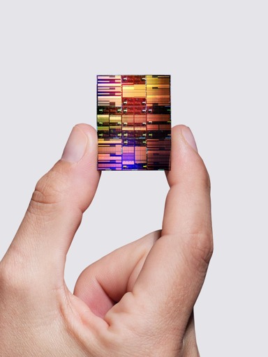
I’d say it’s more an unfortunate consequence of confusing industry terminology. Sub-nanometer refers to the process, not the finished size of the chip. Smaller processes can fit more transistors in the same space.
They call it industry terminology, I call it false advertising. They could easily have used transistors per square mm.
The whole industry needs to be corrected.